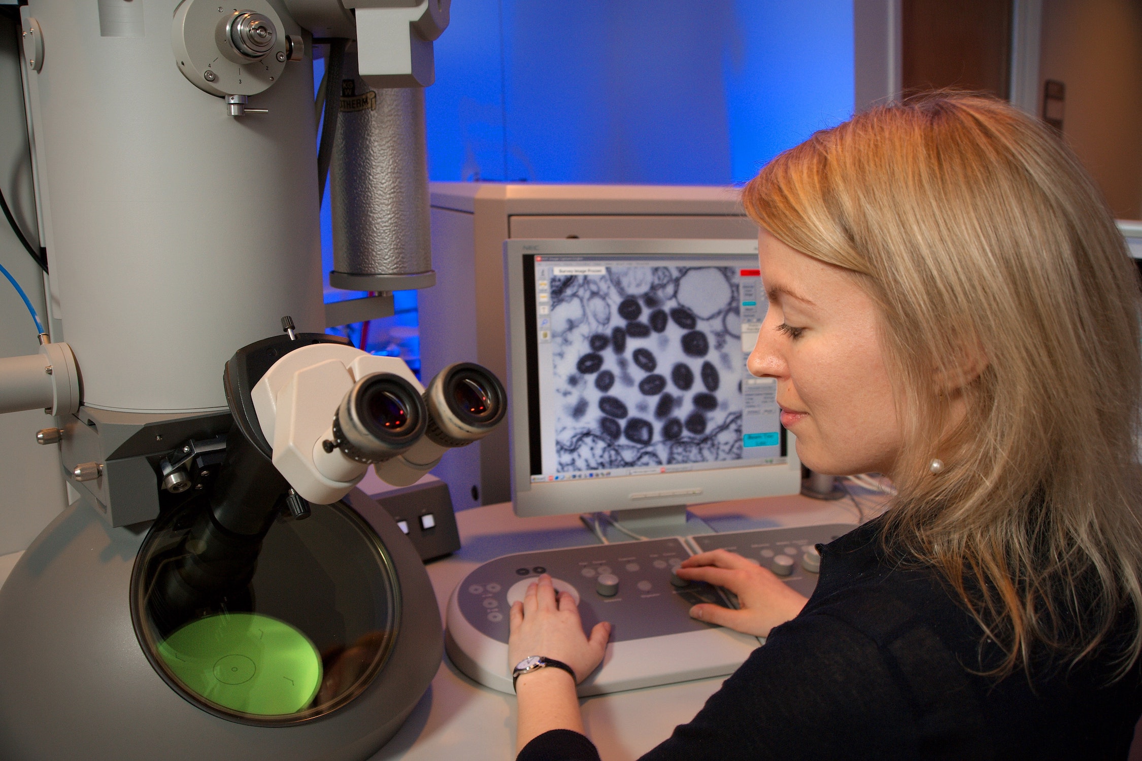
Transmission Electron Microscopy(TEM)
Transmission Electron Microscopy, or TEM analysis, provides high-resolution imaging useful for evaluating all solid materials for Surface and Interface quality and roughness, Defect Type and Density in Semiconductor materials, contaminants or corrosion. This technique in which a beam of electrons is transmitted through a specimen to form an image. The specimen is most often an ultrathin section less than 100 nm thick or a suspension on a grid. An image is formed from the interaction of the electrons with the sample as the beam is transmitted through the specimen.
Through CAS you can have access to TEM-STEM and dedicated AC-STEM, both with EDX and EELS.
TEM/STEM Capabilities:
- Morphology and Surface structure
- Crystal structure: Atomic resolution imaging, electron diffraction
- Chemical Information: Fine probe EELS, EDS, atomic res mapping
- Atomic Bonding: ELNES (Energy-Loss Near Edge Structure) with a high energy resolution
- EPI Layer analysis